- 您现在的位置:买卖IC网 > Sheet目录3818 > PIC18F4620-I/ML (Microchip Technology)IC MCU FLASH 32KX16 44QFN
1996 Microchip Technology Inc.
DS30412C-page 53
PIC17C4X
9.0
I/O PORTS
The PIC17C4X devices have five I/O ports, PORTA
through PORTE. PORTB through PORTE have a corre-
sponding Data Direction Register (DDR), which is used
to congure the port pins as inputs or outputs. These
ve ports are made up of 33 I/O pins. Some of these
ports pins are multiplexed with alternate functions.
PORTC, PORTD, and PORTE are multiplexed with the
system bus. These pins are congured as the system
bus when the device’s conguration bits are selected to
Microprocessor or Extended Microcontroller modes. In
the two other microcontroller modes, these pins are
general purpose I/O.
PORTA and PORTB are multiplexed with the peripheral
features of the device. These peripheral features are:
Timer modules
Capture module
PWM module
USART/SCI module
External Interrupt pin
When some of these peripheral modules are turned on,
the port pin will automatically congure to the alternate
function. The modules that do this are:
PWM module
USART/SCI module
When a pin is automatically congured as an output by
a peripheral module, the pins data direction (DDR) bit
is unknown. After disabling the peripheral module, the
user should re-initialize the DDR bit to the desired con-
guration.
The other peripheral modules (which require an input)
must have their data direction bit congured appropri-
ately.
Note:
A pin that is a peripheral input, can be con-
gured as an output (DDRx<y> is cleared).
The peripheral events will be determined
by the action output on the port pin.
9.1
PORTA Register
PORTA is a 6-bit wide latch. PORTA does not have a
corresponding Data Direction Register (DDR).
Reading PORTA reads the status of the pins.
The RA1 pin is multiplexed with TMR0 clock input, and
RA4 and RA5 are multiplexed with the USART func-
tions. The control of RA4 and RA5 as outputs is auto-
matically congured by the USART module.
9.1.1
USING RA2, RA3 AS OUTPUTS
The RA2 and RA3 pins are open drain outputs. To use
the RA2 or the RA3 pin(s) as output(s), simply write to
the PORTA register the desired value. A '0' will cause
the pin to drive low, while a '1' will cause the pin to oat
(hi-impedance). An external pull-up resistor should be
used to pull the pin high. Writes to PORTA will not affect
the other pins.
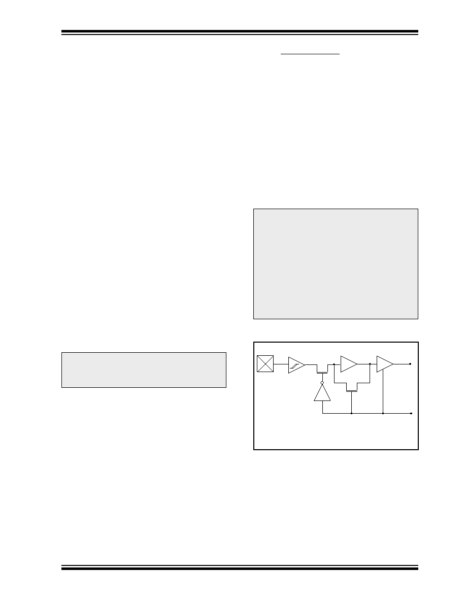
FIGURE 9-1:
RA0 AND RA1 BLOCK
DIAGRAM
Note:
When using the RA2 or RA3 pin(s) as out-
put(s), read-modify-write instructions (such
as BCF, BSF, BTG) on PORTA are not rec-
ommended.
Such operations read the port pins, do the
desired operation, and then write this value
to the data latch. This may inadvertently
cause the RA2 or RA3 pins to switch from
input to output (or vice-versa).
It is recommended to use a shadow regis-
ter for PORTA. Do the bit operations on this
shadow register and then move it to
PORTA.
Note: I/O pins have protection diodes to VDD and VSS.
DATA BUS
RD_PORTA
(Q2)
This document was created with FrameMaker404
发布紧急采购,3分钟左右您将得到回复。
相关PDF资料
PIC24HJ256GP210-I/PT
IC PIC MCU FLASH 128KX16 100TQFP
PIC24HJ128GP310A-I/PF
IC PIC MCU FLASH 128KB 100-TQFP
DSPIC33FJ128GP310-I/PF
IC DSPIC MCU/DSP 128K 100TQFP
PIC16C66-20I/SO
IC MCU OTP 8KX14 PWM 28SOIC
DSPIC33FJ128MC510-I/PT
IC DSPIC MCU/DSP 128K 100TQFP
PIC16C66-20I/SP
IC MCU OTP 8KX14 PWM 28DIP
PIC18LF2620-I/SP
IC MCU FLASH 32KX16 28SDIP
PIC16F877-04I/P
IC MCU FLASH 8KX14 EE 40DIP
相关代理商/技术参数
PIC18F4620-I/P
功能描述:8位微控制器 -MCU 64KB 3968 RAM 36 I/O RoHS:否 制造商:Silicon Labs 核心:8051 处理器系列:C8051F39x 数据总线宽度:8 bit 最大时钟频率:50 MHz 程序存储器大小:16 KB 数据 RAM 大小:1 KB 片上 ADC:Yes 工作电源电压:1.8 V to 3.6 V 工作温度范围:- 40 C to + 105 C 封装 / 箱体:QFN-20 安装风格:SMD/SMT
PIC18F4620-I/P
制造商:Microchip Technology Inc 功能描述:IC 8BIT FLASH MCU 18F4620 DIP40
PIC18F4620-I/PT
功能描述:8位微控制器 -MCU 64KB 3968 RAM 36 I/O RoHS:否 制造商:Silicon Labs 核心:8051 处理器系列:C8051F39x 数据总线宽度:8 bit 最大时钟频率:50 MHz 程序存储器大小:16 KB 数据 RAM 大小:1 KB 片上 ADC:Yes 工作电源电压:1.8 V to 3.6 V 工作温度范围:- 40 C to + 105 C 封装 / 箱体:QFN-20 安装风格:SMD/SMT
PIC18F4620-I/PT
制造商:Microchip Technology Inc 功能描述:IC 8BIT FLASH MCU 18F4620 TQFP44
PIC18F4620T-I/ML
功能描述:8位微控制器 -MCU 64KB 3968 RAM 36 I/O RoHS:否 制造商:Silicon Labs 核心:8051 处理器系列:C8051F39x 数据总线宽度:8 bit 最大时钟频率:50 MHz 程序存储器大小:16 KB 数据 RAM 大小:1 KB 片上 ADC:Yes 工作电源电压:1.8 V to 3.6 V 工作温度范围:- 40 C to + 105 C 封装 / 箱体:QFN-20 安装风格:SMD/SMT
PIC18F4620T-I/PT
功能描述:8位微控制器 -MCU 64KB 3968 RAM 36 I/O RoHS:否 制造商:Silicon Labs 核心:8051 处理器系列:C8051F39x 数据总线宽度:8 bit 最大时钟频率:50 MHz 程序存储器大小:16 KB 数据 RAM 大小:1 KB 片上 ADC:Yes 工作电源电压:1.8 V to 3.6 V 工作温度范围:- 40 C to + 105 C 封装 / 箱体:QFN-20 安装风格:SMD/SMT
PIC18F4680-E/ML
功能描述:8位微控制器 -MCU 64KB 3328 RAM w/ECAN RoHS:否 制造商:Silicon Labs 核心:8051 处理器系列:C8051F39x 数据总线宽度:8 bit 最大时钟频率:50 MHz 程序存储器大小:16 KB 数据 RAM 大小:1 KB 片上 ADC:Yes 工作电源电压:1.8 V to 3.6 V 工作温度范围:- 40 C to + 105 C 封装 / 箱体:QFN-20 安装风格:SMD/SMT
PIC18F4680-E/P
功能描述:8位微控制器 -MCU 64KB 3328 RAM w/ECAN RoHS:否 制造商:Silicon Labs 核心:8051 处理器系列:C8051F39x 数据总线宽度:8 bit 最大时钟频率:50 MHz 程序存储器大小:16 KB 数据 RAM 大小:1 KB 片上 ADC:Yes 工作电源电压:1.8 V to 3.6 V 工作温度范围:- 40 C to + 105 C 封装 / 箱体:QFN-20 安装风格:SMD/SMT